Tests with communication PCB connected to Controller PCB
Because we have now connection between communication PCB and Controller PCB, we can do a few tests:
- Check all Power supplies on all the chips
these were OK
- Check the fan-output
pushing on the Fan button in the right low corner of the PC software application, should activate the Fan, but no Fan yet
connected, so check the Voltage on the negative pin. Should become zero. The other pin is Vcc12 (13.8V)
- Connect 2.2 kOhm resisters between the plus and rel-on and rel-off pins (green connectors at the left upper corner of the PCB)
of all 4 relays outputs. Push the Rel 1,2,3,4 buttons at the right lower corner of the PC application and look whether the voltages
are getting a negative pulse, which means that the relays is shortly activated.
What I notices was, that for relays 1 button ON (light green) gave a negative pulse on the Ext 1 ON output, meaning a activation of
the ON relays. On the relays 2,3, and 4 it is vice versa. A button ON gives a negative pulse on the Rel 2,3 and 4 OFF output.
This is not consistent but not really important .
Also I saw that the negative pulse comes on all outputs which are PUT active, AND the ones that are ALREADY active. For example
If relays 4 is ON, the Rel 4 ON output will also get a negative pulse (again) when you push another button to ON or OFF (for
buttons activating the same driver IC). This is no problem of course, but should not be necessary. Maybe the idea of Norbert was
that in the software he keeps the status of the driver chip (all 8 bit values) in a parameter and send this byte to the chip after each
change. No problem, just good to know.
The working of the shift bits:
If a button is pushed for a capacitor, or a inductor, or one is pushed for controlling the configuration of the C- or L-banks, the micro controller is sending serially 8x8bits from the DATA output of pin 18. These 8 bytes of 8 bits data are shifted into the 8 output drivers (MIC5941YN). One data pulse is about 5 microseconds. Between each byte there is a little pause of about 2.5 microseconds. This is controlled by the system clock signal on pin 19 (SCLK). The SCLK signal is short, about 300nS. The whole train of pulses is about 420 microseconds. After the shift is done all driver IC's have the data in there shift register, but the output is not yet pushed to the latches. This is done by the Strobe signal (pin 20, STRB, about 2 microseconds) and the 8 /OE signals (/OE0 - /OE8). '/OE' is output enabled. So /OE means a negative pulse to enable the buffer content to the output. The pulse is about 30 MILLIseconds. This is enough to get the relays activated.
The DATA bits from the micro controller are high when the push button is dark. This gives a high on the output, causing no current through the relays. So nothing happens. If making the button light green. Current flows through the relay and activated the C, L or other connection. Look at the pictures below.


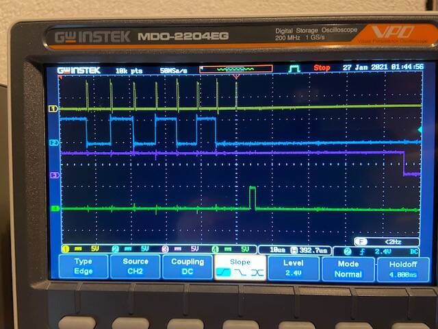
In the left photograph we see the big picture. Yellow shows a whole bunch of clock signals, the blue are the data. The green is the strobe, and the purple is the /OE. In the right photograph the picture is blown up so you see the whole 64 bits of data to be shifted into the 8 buffer IC's. Then the strobe comes in and after that the /OE signal.
The detailed timing of the last byte to be shifted in the most right driver IC is shown in the third picture.
You see 8 pulses of the clock. The last two of them are shifting zero's into the register. Before that three sequences of one-zero.
So in the register we have now 01010100. The green strobe latches the data into the latch buffers. After that the purple negative pulse is passing the value to the output for driving the relays.
To measure these signals, I connected the CapacitorsPCB to the controller PCB with relays and capacitors C2,4,5 soldered on it.
Now we can measure these activities on all 8 driver IC's.
Create Your Own Website With JouwWeb